AD9525 Low Jitter Clock Generator Eight LVPECL Outputs
Product Details
The AD9525 is designed to support converter clock requirements for long-term evolution (LTE) and multicarrier GSM base station designs.
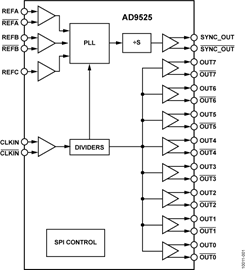
The AD9525 provides a low power, multioutput, clock distribution function with low jitter performance, along with an on-chip PLL that can be used with an external VCO or VCXO. The VCO input and eight LVPECL outputs can operate up to a frequency of 3.6 GHz. All outputs share a common divider that can provide a division of 1 to 6.

The AD9525 offers a dedicated output that can be used to provide a programmable signal for resetting or synchronizing a data converter. The output signal is activated by a SPI write.
The AD9525 is available in a 48-lead LFCSP and can be operated from a single 3.3 V supply. The external VCXO or VCO can have an operating voltage of up to 5.5 V.
The AD9525 operates over the extended industrial temperature range of −40°C to +85°C.
Applications
- LTE and multicarrier GSM base stations
- Clocking high speed ADCs, DACs
- ATE and high performance instrumentation
- 40/100Gb/s OTN Line Side Clocking
- Cable/DOCSIS CMTS Clocking
- Test and Measurement
Features and Benefits
- Integrated ultra low noise synthesizer
- 8 differential 3.6 GHz LVPECL outputs and 1 LVPECL or 2 CMOS SYNC Outputs
- 2 differential reference inputs and 1 single-ended reference inputs